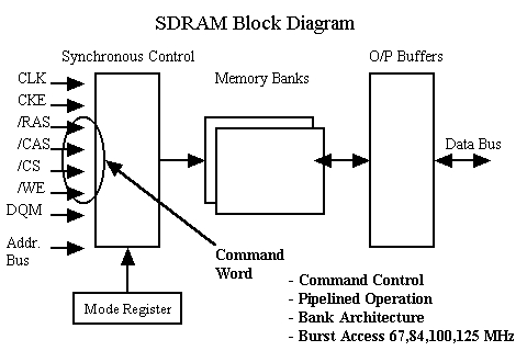
Clock: One of the key differences between SDRAMs and conventional DRAMs is that all operations in the SDRAM are synchronised to a clock signal. This makes the control interface much simpler and eliminates the need to generate pseudo analog RAS and CAS signals which are required for conventional asynchronous DRAMS. It also means that the parts are easier to manufacture than comparable asynchronous parts. An SDRAM for example will have approximately 5 ns faster RAS access time than an asynchronous part made on the same technology.
Command Control: SDRAMs are controlled by commands which are input in the form of a 4-bit command word.
Mode Register: A mode register is included on chip which is used to configure basic device operation. The parameters which are set up are Burst Length, Burst Type and CAS Latency. Usually the mode register is set up once at power up.
Bank Architecture: In an SDRAM the memory array is divided into 2 or more banks. This allows one bank to be precharged while the other is being accessed. This totally eliminates precharge latency and effectively allows bandwidth to be increased. It also means that the granularity (upgrade step) is reduced, which is particularly significant at memory densities of 16 Mbit and upwards.
Pipelined Operation: SDRAMs employ a 3 stage pipeline scheme which allows new memory accesses to be initiated before the preceding access has been completed. When the pipeline is full data can be accessed on every* clock cycle. This along with the burst mode access makes a major contribution to improving the data transfer performance.
*For 1N access rule. For 2N access rule data can be accessed on every second clock cycle.
Burst Mode: SDRAMs incorporate a burst counter on-chip which can be used to increment column addresses for very fast burst access. The burst length and burst type (sequential or interleaved) can be selected by programming the mode register.
![]()