![]()
PROCESSING NODE
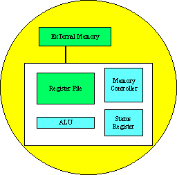
Each Processing Node is composed of a JMILLE floating point processor,
attached to a SDRAM local memory. The Memory Controller inside
Jmille generates addresses for the External Memory summing up a Global Address
given by Tmille and a Local Address computed by Jmille itself. This way each
APEMille Processing Node is able to generate a different Memory Address.
The five addresses needed by the Multiport Register File are fixed by our
compiler at compile time, and therefore distributed to Jmille inside the
Program Word. This is obtained by means of our VLIW (Very Long Instruction
Word) compiling technology.
Each Processing Node generates Status Signals (Global conditions, Exceptions
etc.). These Status Signals are collected into a Global Status Return managed
by the Control System. This connection allows the Control System to execute
flow control instructions based on simultaneous logical conditions produced
by the set of Processing Nodes. The instruction word read by JMILLE specifies
the set of addressed location inside the large multiport Register File
internal to JMILLE, and controls the Arithmetic Devices inside the processing
node. Moreover it specifies Local Conditional Operation, Local Addressing
functions, and Special Arithmetic function calculations to be performed
by JMILLE.
![]()